Find the right camera for semiconductor inspection
Every application has its individual requirements. We know how to help you find the best camera solution for your application.
The requirements for semiconductor inspection systems are increasing in line with technological progress. Ever smaller structures into the deep nanoscale and increased demands on quantities and quality also require ever higher resolutions, faster frame rates and new inspection methods.
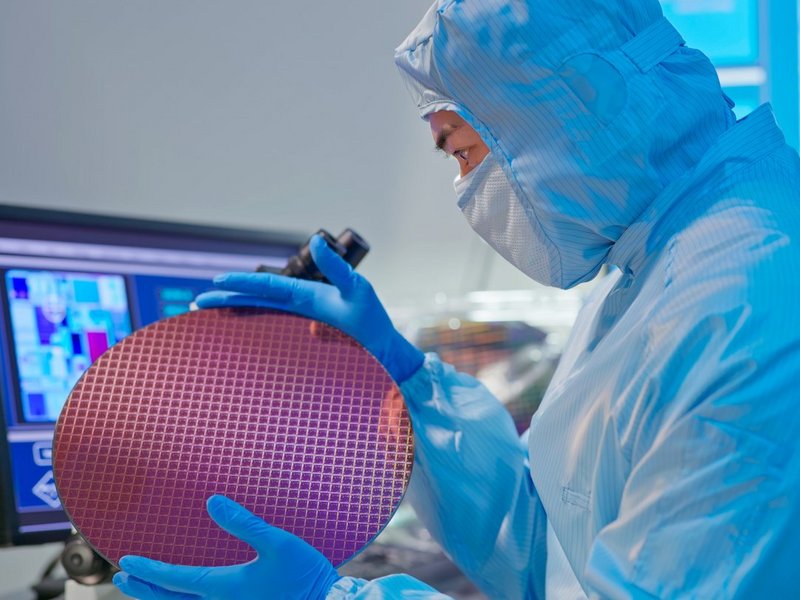
Innovative Wafer Inspection systems enable the detection of surface, material, and process defects of bare, epitaxial, patterned, and diced wafers over the full manufacturing process.
These systems apply automated optical inspection (AOI) including 2D and 3D measurements with high-accuracy and repeatability for MEMS, advanced packaging, RDL, bumps etc. to ensure that a certain yield can be confirmed and maintained.
Often more than 500 steps are needed in the manufacturing process of semiconductor wafers. Consequently, the earlier a defect is detected in the process, the less effort and therefore costs are wasted in subsequent steps.
When choosing a camera for semiconductor inspection, the following aspects can be of relevance:
- High spatial resolution imaging for detecting even the smallest defects and for the alignment of layers with the highest levels of accuracy
- Scalable and flexible solutions by supporting different sensors (in terms of resolution and pixel size) and sensor cooling options, as well as camera interfaces
- State-of-the art sensors running at high frame rates for increasing production throughput
- Active sensor cooling via TEC for ensuring reproduceable imaging results
- Plug & Play feeling when setting up the image processing system enabled by versatile SDK and driver


Various cooling, housing and interface options


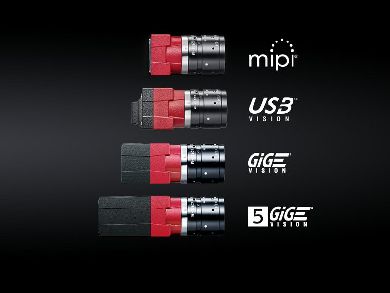
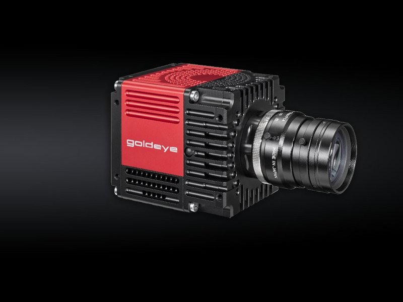
Allied Vision offers the most comprehensive SWIR camera portfolio in the market. Ranging from high-end solutions with thermo-electric cooling (TEC) to tec-less boardlevel version camera modules for developing SWaP+C OEM systems. Select between 3 different resolutions (QVGA, VGA, or SXGA) and 5 interfaces (GigE, 5GigE, USB3, CSI-2, or Camera Link) to design a semiconductor inspection system according to your needs.
Based on our sophisticated SWIR camera solutions, we are always open to discussing a tailor-made solution with you, which includes special functionalities or mechanical adjustments, for example. Our experienced technical experts look forward to learning more about your unique OEM needs.
Finding the right camera for your application
Allied Vision has many years of experience in the development of short-wave infrared cameras with InGaAs sensor technology. With this comprehensive expertise, Allied Vision provides optimized cameras with outstanding image quality in terms of homogeneity, dynamics and linearity for a wide range of applications.
Our engineers design digital cameras with a large scope of resolutions, frame rates, bandwidths, interfaces, spectral sensitivities, sensor technologies, and technical platforms.
Back to Infrared & Hyperspectral Imaging